- 您现在的位置:买卖IC网 > Sheet目录338 > LTC3209EUF-2#TRPBF (Linear Technology)IC LED DRIVR QVGA DISPLAY 20-QFN
LTC3209-1/LTC3209-2
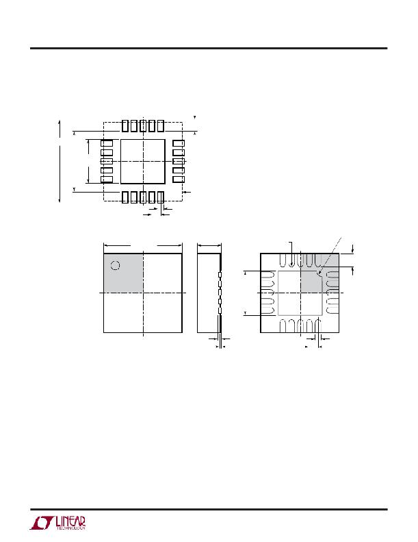
PACKAGE DESCRIPTIO
UF Package
20-Lead Plastic QFN (4mm × 4mm)
(Reference LTC DWG # 05-08-1710)
0.70 ± 0.05
4.50 ± 0.05
3.10 ± 0.05
2.45 ± 0.05
(4 SIDES)
PACKAGE OUTLINE
0.25 ± 0.05
0.50 BSC
RECOMMENDED SOLDER PAD PITCH AND DIMENSIONS
BOTTOM VIEW—EXPOSED PAD
PIN 1 NOTCH
4.00 ± 0.10
(4 SIDES)
0.75 ± 0.05
R = 0.115
TYP
19 20
R = 0.30 TYP
PIN 1
TOP MARK
(NOTE 6)
2.45 ± 0.10
(4-SIDES)
0.38 ± 0.10
1
2
(UF20) QFN 10-04
0.200 REF
0.00 – 0.05
0.25 ± 0.05
0.50 BSC
NOTE:
1. DRAWING IS PROPOSED TO BE MADE A JEDEC PACKAGE OUTLINE MO-220
VARIATION (WGGD-1)—TO BE APPROVED
2. DRAWING NOT TO SCALE
3. ALL DIMENSIONS ARE IN MILLIMETERS
4. DIMENSIONS OF EXPOSED PAD ON BOTTOM OF PACKAGE DO NOT INCLUDE
MOLD FLASH. MOLD FLASH, IF PRESENT, SHALL NOT EXCEED 0.15mm ON ANY SIDE
5. EXPOSED PAD SHALL BE SOLDER PLATED
6. SHADED AREA IS ONLY A REFERENCE FOR PIN 1 LOCATION
ON THE TOP AND BOTTOM OF PACKAGE
320912fa
Information furnished by Linear Technology Corporation is believed to be accurate and reliable.
However, no responsibility is assumed for its use. Linear Technology Corporation makes no represen-
tation that the interconnection of its circuits as described herein will not infringe on existing patent rights.
19
发布紧急采购,3分钟左右您将得到回复。
相关PDF资料
LTC3210EPD-1#TRPBF
IC LED DRVR WHITE BCKLT 16-UTQFN
LTC3210EUD#TRPBF
IC LED DRIVR WHITE BCKLGT 16-QFN
LTC3212EDDB#TRPBF
IC LED DRIVER RGB 12-DFN
LTC3214EDD#TRPBF
IC LED DRIVR WHITE BCKLGT 10-DFN
LTC3215EDD#PBF
IC LED DRIVR WHITE BCKLGT 10-DFN
LTC3217EUD#TRPBF
IC LED DRVR FLASH TORCH 16QFN
LTC3218EDDB#TRPBF
IC LED DRVR FLASH TORCH 10DFN
LTC3219EUD#PBF
IC LED DRIVR QVGA DISPLAY 20-QFN
相关代理商/技术参数
LTC3210
制造商:LINER 制造商全称:Linear Technology 功能描述:MAIN/CAM LED Controller in 3mm × 3mm QFN
LTC3210-1
制造商:LINER 制造商全称:Linear Technology 功能描述:MAIN/CAM LED Controller with 64-Step Brightness Control in 3mm × 3mm QFN
LTC3210-2
制造商:LINER 制造商全称:Linear Technology 功能描述:MAIN/CAM LED Controllers with 32-Step Brightness Control in 3mm × 3mm QFN
LTC3210-3
制造商:LINER 制造商全称:Linear Technology 功能描述:MAIN/CAM LED Controllers with 32-Step Brightness Control in 3mm × 3mm QFN
LTC3210EPD-1#PBF
功能描述:IC LED DRVR WHITE BCKLT 16-UTQFN RoHS:是 类别:集成电路 (IC) >> PMIC - LED 驱动器 系列:- 标准包装:1 系列:- 恒定电流:- 恒定电压:- 拓扑:PWM,切换式电容器(充电泵) 输出数:1 内部驱动器:是 类型 - 主要:背光 类型 - 次要:白色 LED 频率:642kHz 电源电压:2.7 V ~ 5.5 V 输出电压:5V 安装类型:表面贴装 封装/外壳:10-VFDFN 裸露焊盘 供应商设备封装:10-VSON 包装:剪切带 (CT) 工作温度:-30°C ~ 85°C 产品目录页面:1371 (CN2011-ZH PDF) 其它名称:BD1603NUV-E2CT
LTC3210EPD-1#TRPBF
功能描述:IC LED DRVR WHITE BCKLT 16-UTQFN RoHS:是 类别:集成电路 (IC) >> PMIC - LED 驱动器 系列:- 标准包装:1 系列:- 恒定电流:- 恒定电压:- 拓扑:PWM,切换式电容器(充电泵) 输出数:1 内部驱动器:是 类型 - 主要:背光 类型 - 次要:白色 LED 频率:642kHz 电源电压:2.7 V ~ 5.5 V 输出电压:5V 安装类型:表面贴装 封装/外壳:10-VFDFN 裸露焊盘 供应商设备封装:10-VSON 包装:剪切带 (CT) 工作温度:-30°C ~ 85°C 产品目录页面:1371 (CN2011-ZH PDF) 其它名称:BD1603NUV-E2CT
LTC3210EPD-1-PBF
制造商:LINER 制造商全称:Linear Technology 功能描述:MAIN/CAM LED Controller with 64-Step Brightness Control in 3mm × 3mm QFN
LTC3210EPD-1-TRPBF
制造商:LINER 制造商全称:Linear Technology 功能描述:MAIN/CAM LED Controller with 64-Step Brightness Control in 3mm × 3mm QFN
